Schematics are in .JPG format.
Sheet1 - Front end, filter, mixer, IF, regulators 92kB
Sheet2
- Synthesiser 96kB
Drake 2880 Circuit Description
available here
as a Wordpad file - looks better when printed
Introduction
The Drake 2880 downconverter was designed for the reception of Satellite TV signals in the frequency range 2.5 - 2.686GHz, producing an output in the frequency range 222 - 408 MHz. This downconverter was available for some time on the surplus market, and various articles have been written about converting it for use at 2.4GHz for the reception of signals from AO40.
The circuit diagram of the downconverter has never been published by Drake. I have never had any connection with Drake and so the circuit diagram presented here has been reverse engineered by tracing out the connection between all the components. The circuit description is based on experience (which is only one step removed from total guesswork!). This information is intended for guidance only and whilst considerable care has been taken to ensure accuracy, no guarantee can be made that this is a true representation of the actual circuit. It is possible that the circuit of the 2880 downconverter was changed at some point in it's production cycle, and there may be differences and variants. The information presented here is intended for use by the amateur radio community as a whole.
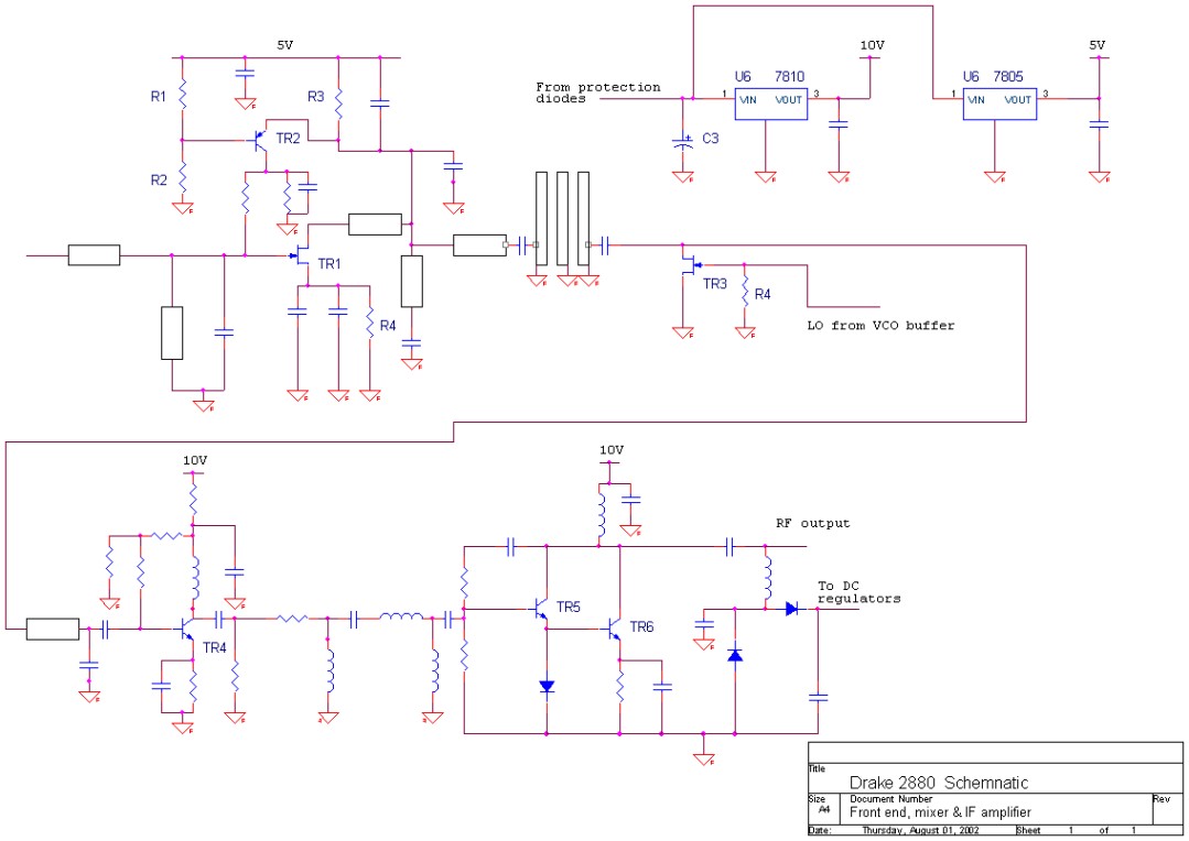
The schematic has been created using ORCAD Lite from Cadence. This version of ORCAD allows for only 60 components per sheet, and so the design is presented on two sheets - sheet 1 shows the RF front end, filter, mixer and IF amplifiers. Sheet 2 shows the Voltage Controlled Oscillator, crystal oscillator and synthesiser components and the power supply. The sheets seem to print out OK on A4 sized paper; they may need to be manipulated for Letter sized paper.
The rectangular boxes on the schematic are printed transmission lines / printed inductors.
Circuit Description
Front end
The input signal is matched to the optimum impedance for the low noise GaAsFET TR1 to give the best noise figure.
TR1 is biased with R4 such that the source voltage is greater than the gate voltage, so the gate-source voltage VGS is always negative which puts the FET into the active region.
The GaAsFET is biased with an active bias network comprising a PNP transistor TR2. The purpose of the active bias circuit is to ensure that the drain current remains constant from device to device and also constant over temperature. The active bias circuit forms a negative feedback function on the gate bias voltage :- the resistors connected to the base of TR2 form a stable potential divider. The current flowing out of the base of TR2 is very small, and the base voltage will effectively be constant. The emitter voltage of TR2 will be at a constant voltage, being approx. 0.6V higher than the base voltage. Now, if the drain current of TR1 was to increase for any reason, the current flowing into the emitter of TR2 would decrease, as the emitter voltage is essentially fixed by the base voltage. Therefore the current flowing out of the collector of TR2 would also decrease, and the voltage at the gate of TR1 would decrease. Therefore the gate voltage of TR2 would decrease, and the gate-source voltage of TR1 would become more negative. This starts to 'turn-off' the FET and the drain current of TR1 will reduce - thus maintaining bias stability.
The GaAsFET has a gain of about 12-18dB; the output signal is matched to a low impedance for the filter.
Filter
The standard filter is a 3 pole interdigital bandpass filter. The centre frequency of this filter is around 2.6GHz, with some loss at 2.4GHz. (Modifying the filter is usually the first thing to do with a standard Drake.) The purpose of the filter is to remove noise at the image frequency; for a standard Drake the image frequency is between 1.87GHz and 2.056GHz.
Mixer
The filtered signal is mixed with an unbalanced mixer. This is believed to be a GaAsFET with no DC bias on the drain. The LO signal is applied to the gate. The FET is then acting as a switch operating at the LO frequency; every half cycle the FET will be 'on', shorting out the input RF signal, and every other half cycle the FET will be 'off', being an open circuit. This creates sum and difference signals at the drain as well as harmonics and unwanted mixing products.
IF amplifier
For the original application the wanted IF signal was between 222 and 408MHz, but the IF amplifier and the filters have enough bandwidth to be able to cope with lower frequencies at 144MHz or 123MHz. The IF signal from the mixer is filtered and then amplified by TR4 which is an NEC 2SC3357 medium power RF transistor. The output from TR4 is filtered and further amplified by TR6 and TR6 which form a Darlington pair. The output is further filtered and applied to the output connector.
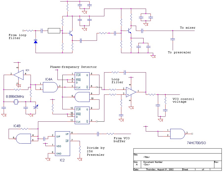
Synthesised Local Oscillator
The Local Oscillator signal is derived from a Phase-Locked Loop Frequency synthesiser.
IC 1 is believed to be an inverting operational amplifier, but this by no means certain. Regardless, IC1 forms an oscillator, the frequency being set precisely by the crystal. The original crystal frequency is 8.8984375MHz. IC 4a is a 74HC00 high-speed CMOS quad 2-input NAND gate. IC4a acts as a buffer for the oscillator. The output of IC4a is the reference signal for the PLL.
The Local Oscillator itself is a Voltage-controlled oscillator (VCO) operating at 256 times the reference frequency; for the original application the VCO frequency was 2278MHz. The VCO consists of a 2SC4093R transistor TR7, in a common collector configuration. The tuned circuit consists of a printed inductor, a capacitor and a varactor diode. The feedback for the oscillator is supplied by the base-emitter capacitance. The frequency of oscillation is determined by the VCO control voltage, which reverse-biases the varactor diode and consequently sets the amount of capacitance in series with the printed inductor, thus setting the resonant frequency.
The output from the VCO is buffered by TR8, another 2SC4093R, and the buffered LO signal is applied to the mixer.
A small sample of the LO signal is applied to the input of the fixed pre-scaler IC5. This divides the frequency of the input signal by 256; the output of which is applied to the Phase-Frequency Detector (PFD) IC3. The other input (reference signal) for the PFD is from the crystal oscillator buffer IC4a.
IC3 is a 74HC74 dual D-type flip-flop, and in conjunction with IC4c forms a classic PFD. A detailed analysis of a PFD is fairly complex, but suffice to say the output (Q or Q' [Q bar]) signal is a series of pulses, and the duty-cycle of the pulses depends on the relative phase of the input signals. A more thorough description of a PFD can be found in the reference [1].
The output pulses from the PFD are smoothed (integrated) to a steady DC signal by the loop filter. The loop filter comprises a low noise op-amp IC2 and associated Rs and Cs. The output from the loop filter is applied to the DC control voltage of the VCO. The PLL acts such that if the VCO signal was to change in frequency, the resultant change in phase at the input to the PLL would cause the mark-space ratio of the output pulses to change, which in turn changes the DC voltage at the output of the loop filter, which pulls the VCO back onto frequency. The loop bandwidth is unknown, but is believed to be quite wide, and so the response time of the loop will be very quick - possibly just a few microseconds.
IC4b is a 'wasted' gate, it is believed that the inputs are connected to the output of the pre-scaler simply to stop them floating. IC4d is unused, the inputs are taken to the 5V supply rail.
Power supply
The DC supply for the downconverter is sent up the output coax. L1 is a radio frequency choke that passes the DC but is an open circuit at the IF frequency. D1 is a reverse-polarity protection diode. D2 stops DC current from flowing out of the downconverter. The 15V input DC supply is regulated to 5V and 10V. The 5V supply is used for the PLL, oscillators and RF amplifier. The 10V supply is used for the IF amplifiers.
Reference
W Hayward & D DeMaw, Solid state design for the Radio Amateur,
ARRL pp48-49. (Good description of Phase-frequency detectors)